

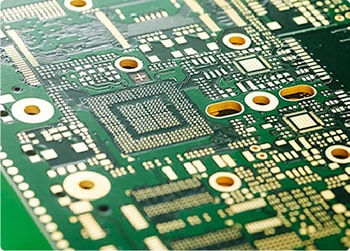

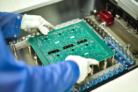
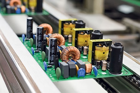










Modern precision electronics continue to pursue miniaturization, high integration and high assembly accuracy. Traditional flat PCBs can no longer meet the special space-avoiding and embedded installation needs of compact chips, sensors and precision modules. This makes Blind Cavity PCB an indispensable structural solution for high-end packaging designs. Different from ordinary through-slot boards, it creates sunken non-through mounting cavities on the PCB surface while protecting internal circuit layers. This structure effectively saves assembly space, improves fitting accuracy and enhances overall structural stability. Even though blind cavity structures deliver obvious application advantages, their manufacturing difficulty is far higher than standard PCBs. Strict process control and precise operational standards are required throughout production to avoid common batch defects.Blind Cavity PCB features non-through recessed cavities tailored for precision electronic assembly. Unlike standard through-slot PCBs, this unique structural board leaves intact inner circuit layers while creating sunken mounting spaces. It is widely specified for precision packaging blind cavity PCB projects, including RF microwave modules, miniature sensing devices and compact wearable electronics. Fabricating qualified blind cavity boards is never simple. It demands strict layered processing and precise depth control, two key factors that separate premium PCB suppliers from ordinary manufacturers.
PCB blind cavity fabrication follows a reverse layered production logic, completely different from conventional PCB grooving. Manufacturers cannot mill cavities after full board lamination. This will easily cut functional inner copper traces and ruin circuit integrity. The correct workflow starts with inner layer fabrication. Teams complete patterning, etching and electrical testing for all internal circuits first. Critical circuit zones near reserved cavity areas get targeted shielding treatment to avoid process damage.
After inner layer validation, multi-layer lamination proceeds with customized parameter settings. Once lamination finishes, rigid board structures take shape. We then adopt combined precision CNC milling and laser ablation to carve blind cavities layer by layer. Progressive machining is essential here. It ensures each cavity stops exactly at the pre-designed dielectric layer, with no through-board penetration. This step defines the basic qualification of custom blind cavity PCB and lays the foundation for subsequent assembly yield.
Depth tolerance control stands as the top technical challenge in mass production. Most factory failures stem from fixed milling parameters. Substrate thickness and lamination compression rates vary slightly per batch. Static program settings easily cause over-milling or under-milling defects. Over-cutting destroys inner circuits directly. Under-cutting leaves residual dielectric material, leading to uneven component seating and poor solder contact. Professional manufacturers dynamically calibrate milling depth based on real board thickness data. Standard qualified blind cavity PCB depth tolerance is strictly controlled within ±0.05mm to eliminate functional risks.
Cavity surface quality is another non-negotiable production detail. Conventional mechanical milling leaves tiny edge burrs and rough base textures. These micro flaws seem trivial, but they heavily impact precision packaging performance. In COB packaging and chip mounting scenarios, burrs create soldering voids and component offset. Most mass production lines only apply basic post-milling cleaning, retaining hidden reliability risks. High-standard processing adds secondary fine grinding and plasma cleaning. This removes all residual burrs and smooths cavity surfaces, delivering flat, clean spaces for high-precision component fitting.
Board warpage is a common yet tricky defect for high-layer blind cavity PCB. Cavity grooving removes partial substrate material, breaking the board’s original structural balance. Asymmetric stress distribution occurs after high-temperature lamination and thermal cycling. Boards easily bend or twist, failing SMT assembly flatness requirements. Many factories lower production speed to reduce defects, which hurts delivery efficiency significantly. The effective solution lies in pre-production stress compensation. Adjusting lamination temperature and pressure curves according to cavity layout balances internal stress and suppresses board deformation fundamentally.
Internal cavity surface treatment requires targeted process optimization too. The semi-enclosed recessed structure blocks liquid flow during plating and solder mask coating. Uniform treatment becomes difficult under standard process parameters. Common defects include uneven gold plating thickness, local solder mask peeling and residual chemical stains. These issues do not affect initial electrical testing. They gradually trigger oxidation, poor solderability and long-term device failure in actual service. Optimized low-flow spraying and segmented plating processes ensure full, uniform coating inside every blind cavity, stabilizing long-term environmental resistance.
Many production failures occur due to ignored structural design details. Irregular cavity shapes, overly narrow transition spacing and sharp-angle traces concentrate structural stress. Under repeated vibration and temperature cycling, cavity edges easily crack, and internal traces may fracture. For high-reliability products, designers must reserve reasonable transition zones and adopt rounded corner processing for cavities. This simple but effective optimization disperses stress and greatly extends the board’s service life.
In short, high-precision blind cavity PCB manufacturing relies on systematic process control, not just basic grooving capability. Depth calibration, surface finishing, stress balance and surface treatment all determine final product quality. Every loose processing detail will trigger batch defects in mass production. Mastering these core technical points is the key to delivering stable, high-yield blind cavity PCBs for high-end industrial, medical and automotive precision electronic applications.