










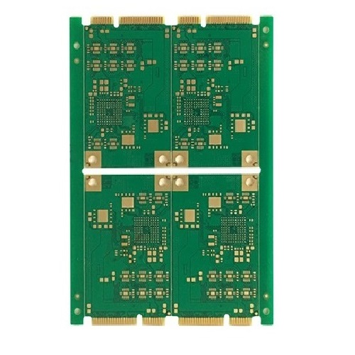
Making a gold finger PCB for tablet motherboards is never as straightforward as a standard board. Most shops run into small, stubborn issues right from the lamination step, and those little flaws can kill connector performance later on.
ANPSE have to lock in the stackup first, usually signal-ground-signal-power-ground-signal, that’s the go-to layout for most tablet builds. But even with that setup, the gold finger plating process demands extra care. The hard gold layer needs to hit at least 1μm thickness, no thinner, or repeated insertions will wear right through it in under 500 cycles.
A lot of manufacturers mess up the tie-bar placement, too. If you run the plating bus too far from the gold finger pads, current distribution goes lopsided, and you end up with uneven gold thickness across the whole edge. Solder mask bleeding onto the fingers is another common headache. You can’t leave any resist residue there, or it blocks electrical contact completely when the tablet slots into its dock or accessory port.
Then there’s the bevel step. 30 degrees is the sweet spot for tablet motherboards, not too sharp, not too flat. Get the angle wrong, and users will fight to plug the board in, or worse, scratch the female connector every single time. Even tiny edge burrs left after chamfering can catch on the slot and peel gold right off the pad.
We’ve seen so many cheap 6-layer gold finger PCB runs fail XRF testing, with gold thickness dipping below 0.3μm on half the fingers. That’s why good shops run full insertion cycle wear testing, nickel-gold adhesion checks, and full AOI scans before shipping any tablet motherboard PCB. Skipping those steps turns a simple component into a costly field failure that no brand wants to deal with.
If you’re sourcing 6 layer PCB for tablet motherboard, never cut corners on gold finger quality — it’s the tiny detail that makes or breaks long term device reliability.


