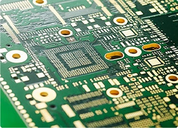
Features of PCBAMake HDI PCB
If you are developing complex electronic products, you need durable, reliable, and high-performance HDI PCBs. With PCBAMake’s advanced HDI manufacturing capabilities, we deliver customized solutions tailored to your specific needs.
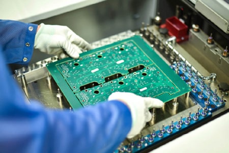
Since 1996, PCBAMake has been committed to supporting innovation and meeting the challenges of increasingly sophisticated technologies. One of our core values is uncompromising quality in every circuit board we produce. To ensure this, we apply rigorous quality control measures at every stage of the manufacturing process, including:
Contact us for a quote