Generic selectors
Exact matches only
Search in title
Search in content
Post Type Selectors
  • Home
  • Quality
  • Blogs
  • Contact Us

What is PCBA testing?

PCBA testing is a critical quality control process that validates the functionality, reliability, and manufacturability of assembled circuit boards. It involves a series of electrical, functional, and environmental checks to detect defects such as short circuits, open connections, component failures, or firmware issues before mass production.

Our strengths in PCBA Testing——Prevents Costly Failures

  • Visual inspection: general quality check.
  • FAI: full quality check applied to the first PCB to pass through all stages of production.
  • X-ray Inspection: checks for BGAs, QFN and bare circuit boards.
  • AOI Testing: checks for solder paste, 0201 components, missing components and polarity.
  • 3D AOI Testing: checks for missing and misplaced SMT components in three dimensions.
  • 3D SPI Testing: measures the precise volume of solder paste for SMT assembly.
  • ICT (In-Circuit Test): Precision Electrical Validation
  • Functional test: (Following your test procedures)

Online Testing (ICT)

In-Circuit Test (ICT) – Precision Electrical Validation

What it checks:

  • Short circuits, open connections
  • Incorrect component values (resistors, capacitors, etc.)
  • Missing or misaligned parts

Key Advantages:

  • High Accuracy – Detects even minor electrical deviations.
  • Fast & Scalable – Ideal for high-volume production.
  • Early Defect Detection – Reduces rework costs.
Online Testing ICT

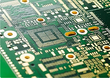
Advantages of SPI (Solder Paste Inspection) – Precision Solder Control

SPI is the first line of defense in SMT production, ensuring perfect solder paste deposition before components are placed. By catching printing defects early, it significantly improves first-pass yield and reduces costly post-reflow repairs.

What it checks:
  • Solder paste volume, height, and coverage
  • Misprints, bridging, or insufficient deposition
  • Stencil alignment accuracy
Key Advantages:
  • Prevents SMT Defects Early – Catches paste issues before reflow, reducing rework.
  • 3D Measurement Technology – Accurately analyzes paste thickness and shape.
  • Process Optimization – Provides data to fine-tune stencil design and printing parameters.
  • High-Speed Inspection – Scans boards in seconds without slowing production.
SPI Testing Process
Automated Optical Inspection

Automated Optical Inspection (AOI) – High-Speed Defect Detection

What it checks:
  • Solder joint quality (bridges, voids, insufficient solder)
  • Component placement (misalignment, polarity errors)
  • Surface defects (scratches, contamination)
Key Advantages:
  • Non-Contact & Fast – Scans boards in seconds.
  • Consistent & Repeatable – Eliminates human error.
  • Works with Miniature Components – Detects defects in 01005-sized parts.

X-Ray Inspection – Hidden Defect Detection

What it checks:
  • Voids, cracks, or misalignment in internal connections
Key Advantages:
  • See Through Components – Inspects what AOI can’t.
  • Critical for High-Reliability Products – Medical, automotive, aerospace.
X-Ray Inspection

Environmental & Reliability Testing – Stress Testing for Durability

What it checks:
  • Temperature cycling (-40°C to +125°C)
  • Vibration, shock, humidity resistance
  • Long-term operational stability
Key Advantages:
  • Simulates Harsh Conditions – Ensures survival in extreme environments.
  • Reduces Field Failures – Critical for automotive, military, and medical devices.
Environmental Testing
Email
Email: 666666@qq.com
Email
Skype: 666666@qq.com
Wechat
WhatsApp QR Code
WhatsApp
WhatsApp QR Code
(0/8)