Design for Manufacturing
DFM is the process of arranging a PCB topology with the manufacturing process in mind. With this design mentality, the PCB layout topology is intended to mitigate problems that typically occur during the fabrication and assembly processes, including:
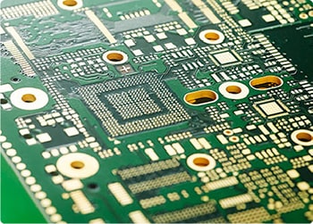
Slivers and islands:
Pieces of free-floating copper on a PCB layer can cause issues in a PCB design, which tends to happen when a design includes several areas with small islands of copper between traces.
Solder bridges:
When traces and pins are placed too close together and a solder mask isn't used in a design, solder can create bridges between pins, causing shorts and corrosion along with other issues.
Copper to edge:
Sometimes, the copper on a PCB is too close to the edge of the board, causing shorts to occur during the etching process when an electrical current is applied. DFM tests should be implemented early to reduce overall costs.
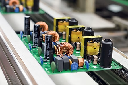
Design for Assembly
For any PCB assembly, it's essential to attach components securely to the circuit board. Unfortunately, doing so can be difficult when the design is hard to assemble, which is why DFA is essential. With DFA, the goal is to determine how to design the PCB so that the assembler can complete their job quickly and effectively.
The DFA process includes the following steps:
• Minimize material inputs.
• Choose easily available components.
• Give components an adequate amount of space between each other.
• Apply general standards of PCB design.
• Make markings for components accurate and clear.
Like DFM, DFA tests should be implemented early on in a project design process to minimize production costs and product development time.
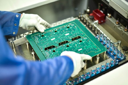
Design for Test
DFT is a type of design that helps make testing more thorough and less costly. Essentially, PCBs designed with DFT in mind are designed to make it easy to detect and locate failures. This way, it’s easier to run tests quickly and accurately, reducing the amount of time needed for testing. For this to work, designers have to know exactly what type of testing methods they’ll be using at each stage of production.
DFT can require a great deal of additional design and engineering effort in the PCB design process, easily making up for the amount of time saved during testing. With faults easier to find, it’s less likely for PCBs with hidden faults to be sent out, reducing the cost of customer dissatisfaction and potential recalls.
Design for Supply Chain
One thing that many designers don’t consider is the life cycle of a product or component. Often, certain components become obsolete during the product life cycle of a PCB, and it becomes more difficult to source that component in a cost-effective way. It’s essential to consider component life cycles when designing new products with DFSC techniques.
Staying aware of life cycles includes talking to an experienced electronics contract manufacturer to determine stock availability and alternate sourcing for the components of a PCB early in the design process. In the long run, this DFSC strategy will help save money by ensuring a long lifespan for a PCB design.