

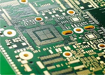
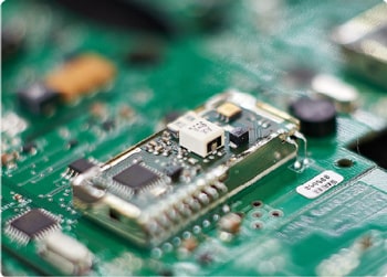










6L HDI rigid-flex PCB is a core high-density circuit solution widely adopted in modern communication hardware. Unlike ordinary rigid-flex boards, its six-layer HDI stacked structure with microvia integration solves the dual pain points of miniaturization and high-frequency signal stability, which are critical for the telecom industry. At ANPSE Tech, we mainly apply this board type to 5G RF modules, base station transceiver units, and portable communication terminals. It effectively optimizes internal wiring space and fixes common signal attenuation issues that plague traditional multi-board connection designs in communication equipment.
Telecom devices demand far stricter layer precision than regular industrial boards, making alignment control vital for 6-layer HDI rigid-flex PCB production. We deploy high-TG FR4 rigid substrates matched with 25μm to 50μm PI flexible film for all communication-grade batches. This material combination delivers stable structural support for RF chip soldering on rigid zones, while flexible sections maintain reliable bending performance for antenna connection parts. We lock layer alignment tolerance within ±0.05mm during DFM pre-review, a key standard to avoid crosstalk and signal deviation in high-frequency communication transmission.
Microvia precision directly decides signal integrity for communication equipment, standing as the key of HDI rigid-flex PCB processing. We use laser drilling to form 0.1mm ultra-fine microvias, ideal for dense routing of 5G high-frequency circuits. The minimum line width and spacing is controlled at 2.5/2.5 mil for flex areas and 4/4 mil for rigid areas, supporting precise layout of RF signal lines and impedance matching circuits. Every microvia undergoes full plasma desmear treatment to eliminate resin residue, ensuring consistent and loss-free signal transmission during long-term telecom device operation.
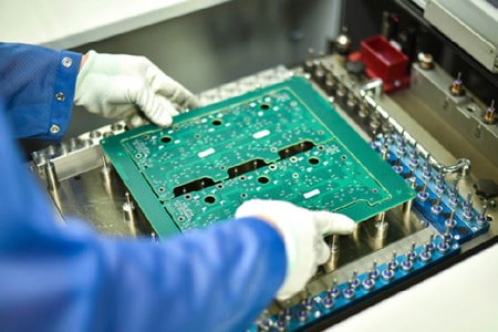
Stable lamination is essential to maintain consistent impedance performance for custom 6L HDI rigid-flex PCB used in communication scenarios. We implement vacuum lamination at 1.5–2.5MPa and 170–190°C, with cooling speed strictly limited to 3–5°C per minute. This steady process prevents board warpage and interlayer delamination, two major causes of unstable RF signal output. We adopt professional no-flow prepreg to prevent resin overflow on flexible antenna zones, keeping the bending structure intact without interfering with high-frequency signal conduction.
We add exclusive communication-oriented reliability tests for finished 6L HDI rigid-flex PCB. Besides standard 100% AOI inspection and electrical testing, we simulate real telecom working environments. Boards undergo 10,000+ times of bending tests with a 20x board-thickness bending radius, adapting to frequent folding and vibration of base station antenna connectors and portable communication devices. We also verify high-frequency signal stability to ensure no signal drift or attenuation under continuous high-load operation.
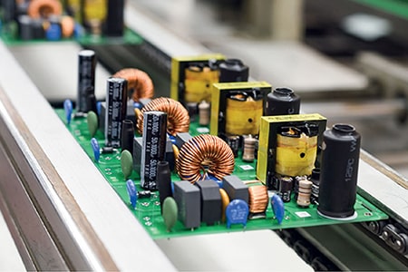
With rich experience serving the communication industry, ANPSE Tech offers professional 6L HDI rigid-flex PCB manufacturing for various telecom devices. Our solutions cover 5G RF modules, base station internal connection boards, and intelligent communication terminal hardware. We support prototype validation and large-scale mass production, tailoring high-reliability rigid-flex boards to meet the high-frequency, miniaturized, and high-stability demands of modern communication electronics.