

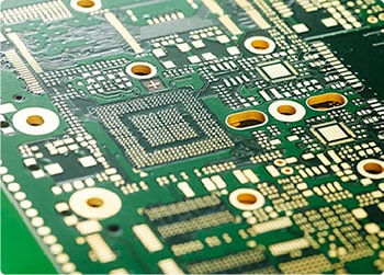
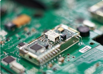
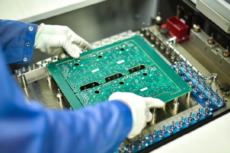










High-density tablet motherboard PCB serves as the core hardware solution for modern thin and light flagship tablet devices. Compared with conventional mid-tier 12-layer circuit boards, premium tablet mainboards need to accommodate extremely complex circuitry within an ultra-compact, slim body. Current high-end tablets integrate multi-channel DDR memory wiring, high-speed GPU signal transmission, 5G internal antenna circuits, and 4K ultra-HD display drive lines on a single tiny board structure. Precision manufacturing for slim tablet circuit hardware is far more demanding than regular consumer PCB production. There are countless subtle process details that can easily trigger performance instability and reduce device service life if not strictly controlled.
Symmetrical stack-up lamination is always a tough bottleneck for ultra-thin high-layer tablet PCBs. Most flagship tablet models require a final board thickness controlled between 0.9mm and 1.1mm. Fitting 16 layers of intricate circuits in such a slim structure inevitably generates concentrated internal stress during production. We always adopt full symmetrical stack-up layouts to evenly disperse pressing pressure and balance structural stress. The layer alignment offset is strictly limited within ±0.02mm, a rigorous standard never required for ordinary multilayer consumer boards. We maintain lamination temperature steadily at 172–180°C with gradual pressure regulation, and set a constant cooling rate of 2°C per minute. Minor stress imbalance will cause subtle micro warpage, which greatly affects later assembly precision and overall tablet fitting effect.
Cascaded microvia fabrication is another tricky technical challenge for high-layer slim tablet motherboards. High-end tablet devices rely heavily on stacked and staggered microvia structures to realize dense cross-layer circuit interconnection. We adopt professional UV laser drilling to produce ultra-fine vias with a minimum aperture of 0.07mm. The microvia aspect ratio is controlled below 0.7:1 all through production, effectively preventing via barrel cracking and open circuit risks. Resin smear is a prevalent defect in high-density multilayer board processing, so we extend plasma desmear treatment to 12–15 minutes for every panel. This process ensures stable via conduction resistance and avoids intermittent circuit failures during long-term daily use of tablet devices.


