

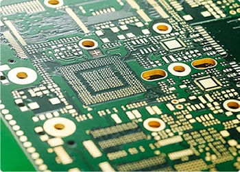
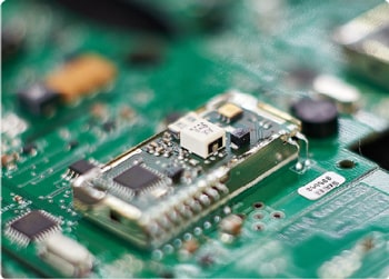
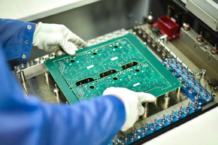










BGA HDI PCB is a core high-density circuit board specially developed for BGA packaged chip mounting. Compared with ordinary multilayer PCBs, this board adopts fine-line circuits, dense pad layouts and stacked microvia structures, perfectly solving the wiring bottleneck of traditional PCBs for high-pin-count BGA chips. Custom BGA HDI PCB supports stable electrical signal transmission while realizing equipment miniaturization, serving as a key carrier for modern precision electronic manufacturing. Its core processing difficulties mainly focus on fine pitch circuit production and microvia fabrication. High-end BGA components come with ultra-narrow pad spacing and dense pin distribution, which cannot be satisfied by conventional PCB manufacturing processes. This board requires ultra-fine line etching and high-precision circuit alignment to prevent short circuits and open circuits caused by dimensional deviation. Meanwhile, stacked microvia alignment and lamination consistency pose great challenges. Tiny position offset during drilling and lamination will lead to poor interlayer conduction and unstable current transmission, directly reducing the assembly yield of BGA chips.
Precision surface processing and flatness control are essential technical guarantees for qualified BGA HDI PCB. Solder mask opening accuracy is critical for dense BGA pad areas. Inaccurate window size and offset openings easily cause solder bridging and insufficient tin plating during SMT soldering. Manufacturers need to strictly control exposure and developing parameters to ensure uniform solder mask openings and smooth pad surfaces, adapting to mass assembly and BGA rework requirements. In addition, strict board warpage control is indispensable for this board. The uneven copper distribution and dense internal wiring of high-density BGA HDI PCB are prone to deformation after multiple high-temperature lamination cycles. Excessive warpage will cause poor fitting and virtual soldering between BGA chips and the board. Optimized lamination pressure, temperature and cooling procedures effectively improve board flatness and fully meet high-precision SMT assembly standards.
High-reliability custom BGA HDI PCB has become the mainstream choice for high-end precision electronic equipment due to its outstanding high-density wiring capability and stable electrical performance. It is widely applied in 5G communication devices, automotive electronic control systems and industrial intelligent equipment, supporting stable operation of high-speed signal circuits. Besides, this board is commonly used in medical precision instruments, high-speed computing hardware and high-end consumer electronic motherboards. It effectively meets the dual demands of equipment miniaturization and high-performance operation, providing reliable circuit support for various sophisticated electronic products.


