

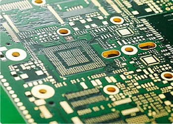
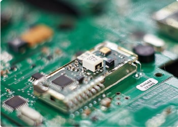
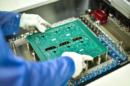
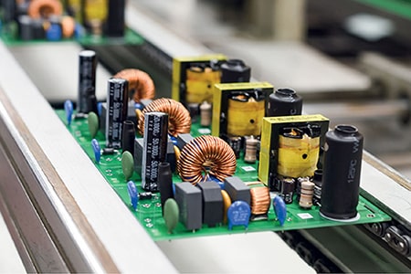








Aluminum Nitride (AlN) PCB features extreme hardness and high brittleness, which makes conventional routing, stamping, and standard mechanical cutting methods completely unsuitable for substrate shaping. Unlike flexible FR-4 PCBs and tough alumina ceramic boards, high thermal conductivity Aluminum Nitride PCB is highly prone to edge chipping, micro-cracks, and layer delamination under rigid mechanical impact. Professional manufacturers rely on mature, low-stress cutting and forming processes tailored for brittle ceramic substrates to ensure dimensional accuracy and long-term circuit reliability. The most widely adopted industrial solutions include laser cutting, diamond blade dicing, and precision wire cutting, each applied according to substrate thickness, outline complexity, and mass production requirements.
Laser cutting for Aluminum Nitride ceramic substrate stands as the primary process for high-precision and complex-shaped AlN PCB forming in modern electronics manufacturing. Manufacturers typically deploy UV and CO₂ laser systems with nitrogen auxiliary cooling to eliminate thermal burns and carbon residues on cutting edges. This non-contact machining method generates zero mechanical stress on AlN substrates, effectively avoiding micro-crack propagation that easily occurs during physical cutting. It excels at processing irregular outlines, tiny groove structures, and miniaturized high-density circuit boards widely used in high-power semiconductor modules and precision optoelectronic devices. For thin Aluminum Nitride PCBs below 3.0mm, laser cutting delivers tight dimensional tolerance and smooth edge quality, eliminating secondary grinding procedures and improving production efficiency significantly.
For standardized mass production with regular straight outlines, diamond blade dicing and precision wire cutting serve as more cost-effective forming alternatives. High-speed diamond dicing machines with thin customized blades process bulk AlN PCB panels steadily, with strictly controlled spindle speed and feed rate to reduce edge chipping. This process fits thick substrate forming and large-volume depaneling of finished circuit panels. Meanwhile, diamond wire cutting uses constant tension and oil-based cooling systems to achieve ultra-smooth cutting surfaces, ideal for high-thickness Aluminum Nitride PCBs that require ultra-high edge flatness. Unlike laser processing, these mechanical precision methods lower equipment costs for mass production while maintaining stable structural integrity, making them ideal for industrial-grade power electronic AlN PCB batches.