










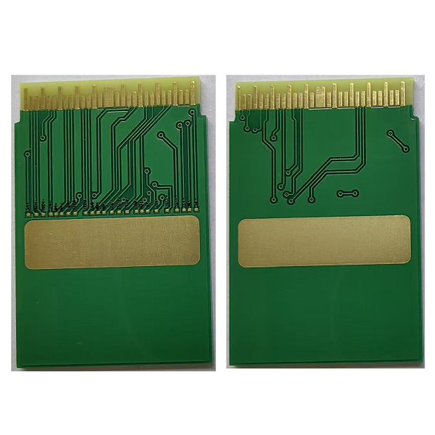
Leiterplatte aus Kupfermünzen is a proven thermal optimization solution for today’s high-density power electronic devices. Standard PCBs rely on thermal vias and surface copper pours to dissipate heat, but these basic structures can barely handle the intense heat flux from IGBT units, high-power LEDs and automotive core power chips. We’ve seen countless customer projects run into identical practical issues. Excess thermal resistance creates stubborn local hotspots, driving up component junction temperatures and speeding up device aging during prolonged high-load operation. As an experienced PCB manufacturer, ANSE Technology leverages a mature embedded copper coin PCB custom process to solve these real-world thermal bottlenecks and deliver reliable, high-efficiency thermal management for high-power hardware.
Most thermal failures in conventional PCB designs trace back to inefficient internal heat conduction paths. FR-4 dielectric material offers very poor thermal conductivity, locking heat inside circuit layers and forming persistent hotspots. Even densely arranged thermal vias fail to fully release accumulated heat, resulting in unstable power output and frequent equipment power derating. For high-current working conditions, traditional PCB structures also lack sufficient current-carrying capacity, triggering severe Joule heating and further exacerbating thermal stress. Our high thermal conductivity copper coin PCB completely reworks the internal heat transfer structure. By embedding high-purity solid copper coins directly beneath heat-generating components, we build straight vertical heat conduction pathways. This bypasses the low-efficiency heat transfer through dielectric layers, cutting overall thermal resistance by 30% to 70% in actual application.
Beyond obvious heat dissipation improvements, our copper coin process addresses critical reliability pain points that puzzle most power electronics designers. Standard thermal-via PCBs often suffer from the popcorn effect, layer delamination and solder joint micro-cracks when exposed to high-temperature reflow and repeated thermal cycling. These defects are extremely risky for automotive electronics and industrial control devices that require up to 10 years of stable service life. We tailor every copper coin embedded PCB for power modules with structural matching optimization. The integrated copper coin structure delivers well-matched thermal expansion with the substrate, easing internal thermal stress effectively. It greatly eliminates board bulging, delamination and solder joint fracture risks during thermal shock tests, boosting mass production yield and long-term device durability significantly.
Mass-producing qualified copper coin PCBs is never easy for ordinary manufacturers. Common flaws include uneven embedding gaps, poor surface coplanarity and exposed copper oxidation, all of which hinder large-scale batch application of high-power products. With years of accumulated experience in high-power precision PCB fabrication, ANSE Technology has built a complete, stable manufacturing workflow for copper coin embedding technology. We use precision CNC grooving and customize depth calibration based on each client’s actual power density requirements. This ensures a zero-gap fit between copper coins and substrate grooves. Only high-purity oxygen-free copper with a thermal conductivity of 401 W/m·K is adopted, guaranteeing consistent and stable heat transfer performance for every finished circuit board.
We’ve developed targeted process specs to eliminate typical copper coin PCB defects entirely. Exclusive segmented pressing and high-temperature aging processes are applied during lamination. Accurate real-time control of pressure and temperature avoids copper coin offset, board warpage and layer misalignment. Subsequent professional surface finishing and anti-oxidation treatment keep copper coin surfaces flat and clean, supporting flawless SMT soldering and assembly. Before delivery, every board undergoes full coplanarity inspection and thermal resistance sampling tests. This strict quality control ensures each batch of power dissipation copper coin PCB fully meets the rigorous standards of long-term high-load operation.
Our optimized copper coin PCB solutions have been widely verified and applied in mass production. Typical scenarios include new energy vehicle ECU modules, industrial inverter power supplies, high-brightness LED lighting systems and 5G RF power amplifier units. For product developers pursuing miniaturization, high power density and long-term reliability, ANSE’s professional copper coin embedding process delivers tangible value. It effectively reduces thermal-related failure rates and cuts post-production maintenance costs. More importantly, it offers a cost-efficient high-performance thermal upgrade, serving as a practical alternative to expensive ceramic substrates for most high-power electronic projects.