

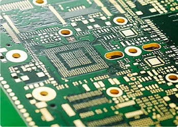

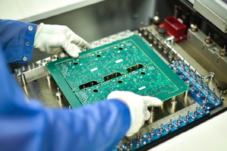
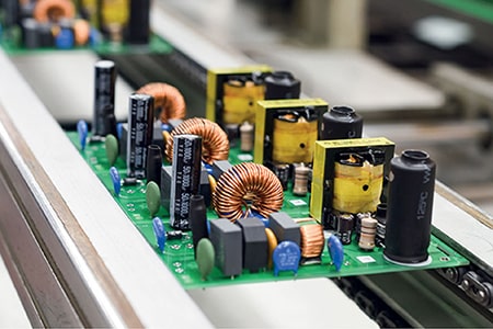










Optical module PCB is the core carrier of all optical transceiver communication equipment. Unlike ordinary industrial circuit boards, these high-speed boards directly support photoelectric signal conversion for SFP, QSFP and OSFP modules. Even tiny manufacturing flaws can cause signal loss, unstable transmission or low photoelectric conversion efficiency in actual operation. At ANPSE Tech, we’ve been optimizing optical module PCB processing for years, focusing on high-frequency stability, precise impedance control and long-term thermal reliability for optical communication scenarios.
Material selection is the first step that separates qualified optical module boards from ordinary PCBs. Standard FR4 substrates cannot meet high-speed transmission demands. We exclusively adopt low-loss high-speed laminates with ultra-smooth SVLP copper foil, controlling surface roughness Rz ≤ 2μm. This effectively reduces high-frequency insertion loss, especially critical for 100G to 800G high-rate optical modules. Before formal production, all substrates undergo constant-temperature baking at 135°C for 3 hours, strictly controlling internal moisture content below 0.1% to avoid board delamination and soldering blistering.
Impedance consistency is the biggest challenge in high-speed optical module PCB fabrication. Optical communication differential circuits require ultra-stable impedance performance. We strictly lock impedance tolerance within ±5%, far tighter than regular PCB standards. The minimum trace and space is controlled at 3mil/3mil to adapt dense high-speed wiring. Every batch undergoes sampling impedance testing during production, calibrating line width and copper thickness in real time to prevent signal distortion during photoelectric transmission.
Drilling and backdrilling precision greatly affects high-speed signal integrity. Stub residues will generate serious signal interference for high-rate optical modules. We control the maximum backdrill stub length below 3mil, and keep drilling hole position tolerance within ±0.05mm. All via holes go through full plasma desmear treatment to eliminate resin residue. The via void rate is strictly controlled below 5%, ensuring stable and unobstructed interlayer signal conduction.
Thermal structure design and processing details are easy to overlook but extremely important. Optical module PCBs work with laser chips and high-power driving components, which generate continuous heat during operation. We arrange dense thermal vias in core heat dissipation areas and adopt 1–2oz thickened copper layers. This structure improves heat conduction efficiency and avoids local overheating that causes optical power attenuation and module performance degradation after long-term operation.
Surface finishing and appearance precision follow strict optical communication industry standards. Most custom optical module PCB orders adopt hard gold plating for connector fingers. We ensure zero exposed nickel, zero scratches and zero surface contaminants. Finished boards pass more than 500 plug-in cycle tests to guarantee stable contact performance for long-term equipment docking. Board warpage is controlled below 0.1%, perfectly matching the assembly precision requirements of optical chips and optical device components.
As a professional manufacturer focusing on communication circuit boards, ANPSE Tech provides reliable optical module PCB manufacturing solutions for data center and optical communication industries. We support prototype verification and mass production of high-speed optical module boards from 100G to 800G. Strict full-process precision control ensures every finished board delivers low loss, stable impedance and excellent thermal performance for commercial optical transceiver devices.