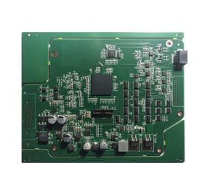

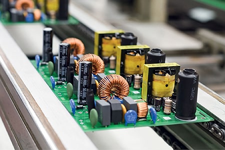










In the fast-evolving landscape of financial technology, the financial communication control PCBA stands as the unsung backbone of secure, uninterrupted transaction systems. From bank terminal networks to high-frequency trading data links, these specialized printed circuit board assemblies are engineered to handle sensitive data transmission, real-time signal processing, and 24/7 operation without compromise. Unlike general-purpose industrial PCBA, a financial communication control board must meet far stricter standards, where a single soldering defect or signal interference can lead to millions in lost transactions or critical data breaches.
When it comes to financial PCBA manufacturing, the first non-negotiable requirement is compliance with global payment card industry and financial security standards. Every production step must align with ISO 27001 for information security, IPC-A-610 Class 3 for high-performance electronics, and local financial regulatory guidelines such as PCI DSS for payment terminal hardware. Most leading fabricators also implement full material traceability for every component, from high-speed differential signal transceivers to isolated power modules, ensuring no counterfeit parts enter the assembly line — a critical safeguard that generic communication control PCBA production rarely enforces at this level.
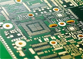
Signal integrity is another make-or-break factor. A typical financial communication control PCBA carries multiple encrypted data lanes running at speeds over 1Gbps, alongside isolated analog sensor channels for line status monitoring. During the PCB layout stage, engineers must apply controlled impedance routing, length matching for differential pairs, and faraday cage shielding around RF communication sections to eliminate electromagnetic interference. Even a 5% deviation in impedance tolerance can cause packet loss in transaction data, leading to failed bank transfers or dropped connections between ATM networks and core data centers.
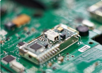
The assembly process for these boards demands far tighter precision than standard consumer electronics manufacturing. For SMT assembly for financial PCBA, manufacturers use high-precision placement machines with ±25μm accuracy for fine-pitch QFP and BGA components, paired with reflow ovens that feature 12+ temperature zones to maintain a perfect thermal profile for lead-free soldering. Many qualified factories also add a selective soldering step for through-hole connectors that handle external network cables, reducing cold solder joint rates to below 0.3% — a benchmark that is nearly impossible to achieve in mass-market PCBA production.
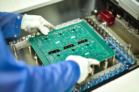
Every completed financial communication control PCBA goes through a three-stage testing workflow before leaving the factory. First, an automated optical inspection (AOI) scans every solder joint and component marking to catch visible defects. Next, an in-circuit test (ICT) verifies all electrical connections, component values, and power isolation performance. Finally, a 72-hour burn-in test under 45°C high-temperature environment runs continuous data transmission simulations, filtering out any boards that might fail prematurely under real-world non-stop operation. This rigorous testing flow is why top financial equipment brands consistently prioritize suppliers with proven experience in secure financial hardware PCBA fabrication over low-cost general electronics shops.
Many project teams new to this space make the mistake of treating a financial communication control PCBA the same as a regular industrial communication board, only to face costly failures after deployment. One frequent error is skipping dedicated ESD protection design on all external communication ports, which leaves the board vulnerable to electrostatic damage during on-site maintenance in bank branches. Another oversight is using standard FR-4 substrate material instead of high-Tg FR-4 with a glass transition temperature over 170°C, which can cause board warpage after months of continuous operation in poorly ventilated server room cabinets.
Working with a manufacturer that has existing certifications for financial communication control board production is the most effective way to avoid these risks. Experienced suppliers already have pre-validated material lists, standardized testing procedures, and full audit trails that meet the strict documentation requirements of financial regulators. This not only cuts down your product certification timeline by 30-40% but also eliminates the hidden costs of reworking batches that fail compliance audits later in the product lifecycle.
As global financial networks continue to shift toward real-time, cloud-connected transaction infrastructure, the demand for high-reliability financial communication control PCBA will only keep rising. For design engineers and procurement managers, the priority is no longer just getting a board assembled at the lowest cost — it is partnering with a fabrication team that understands the unique security, stability, and compliance demands of the financial sector. A well-managed manufacturing process does not just deliver a finished circuit board; it delivers the peace of mind that every transaction passing through it will remain secure, accurate, and online, 365 days a year.