

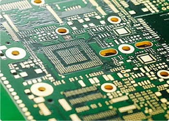

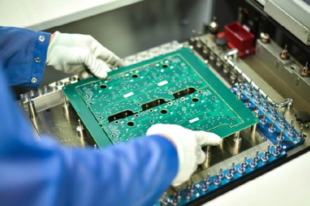










IC Substrate PCB requires far stricter fabrication precision than ordinary commercial PCBs. These specialized boards serve as reliable pad carriers for semiconductor wire bonding and flip-chip chip assembly. High-precision IC substrate pad accuracy is one of the key factors that determine packaging yield, signal stability and overall service life of finished semiconductor devices. Even tiny dimensional errors or position shifts can cause bonding misalignment, solder voids and occasional circuit faults. For ultra-fine pitch, high-density packaging projects, consistent pad tolerance control remains a core focus throughout mass production.
IC substrate PCB pad precision processing relies on full-process coordinated control, with nearly every manufacturing stage impacting final pad quality and consistency. Traditional film exposure, commonly used for standard PCB production, easily creates pattern stretching and distortion. For this reason, premium IC substrates adopt laser direct imaging to deliver sharp, accurate ultra-fine micro pad patterns. After developing and chemical etching, workers perform secondary edge trimming to clear fine burrs and residual copper. Meanwhile, precise thickness management for ENIG and ENEPIG surface finishes avoids oversized pads caused by excessive metal plating, keeping dense pad arrays within stable dimensional tolerance.
Volume production of IC substrates still faces recurring precision risks triggered by subtle process fluctuations. Lamination misalignment ranks among the most frequent issues. Small layer offsets during high-pressure lamination misalign upper and lower layer pads, directly undermining chip assembly accuracy. Uneven etching speed across different panel zones also leads to irregular pad edge shrinkage, resulting in out-of-spec pad sizes. Moreover, repeated high-temperature heating during pressing and surface treatment generates thermal stress and slight board warpage. On high-density packaging IC substrate with compact micro pad layouts, even minimal warpage can create obvious position deviation and lower bonding consistency.
Real mass-production cases fully demonstrate how targeted process tweaks fix pad precision defects and boost overall yield. One typical example is a commercial 0.4mm pitch µBGA IC substrate project designed for mobile AI processor packaging. The project initially struggled with inconsistent pad dimensions and rough pad edges, causing around 7% assembly failure due to inaccurate solder bump alignment. Our engineering team optimized laser exposure positioning parameters and deployed segmented etching calibration for high-density pad zones. After iterative adjustment, pad dimensional tolerance stabilized at ±3μm, lifting mass production packaging yield from 93% to 98.5% steadily.
Another practical case involves high-end DDR5 memory IC substrate manufacturing. This product features ultra-fine 30μm lines and pad structures, with strict requirements for full-panel flatness and uniformity. Early production batches suffered localized pad dishing and uneven plating thickness, which triggered unstable contact resistance and poor high-speed signal transmission performance. The production team upgraded to uniform high-speed copper plating equipment and added real-time thickness monitoring during processing. This improvement controlled full-panel plating variation within 1.2μm, eliminating uneven pad height and fully meeting the strict impedance stability standards for high-frequency memory IC packaging.
Trusted substrate manufacturers adopt systematic precision control measures to maintain stable pad quality for high-end semiconductor applications. Pre-exposure laser calibration completely eliminates pattern positioning errors. Custom etching formulas are configured based on actual pad density and substrate thickness, ensuring uniform etching effects across the entire panel. Segmented temperature control during thermal processing effectively relieves internal stress and minimizes board deformation. These practical, field-verified methods stabilize pad size, flatness and position tolerance, fully catering to the rigorous quality demands of automotive semiconductors, 5G communication ICs and industrial high-precision packaging devices.