

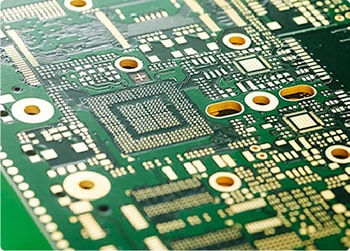
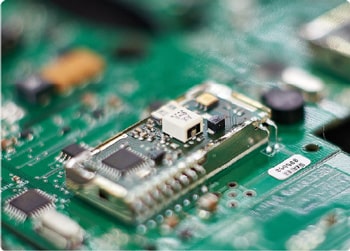
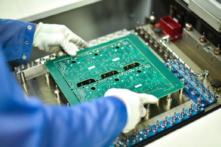
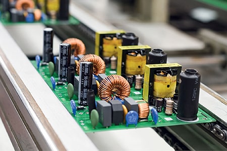










10-layer 2+N+2 HDI PCB is one of the most practical high-density stack-up structures for modern communication and high-speed industrial devices. Unlike standard multilayer HDI boards, its unique 2+N+2 stack-up design features two sequential build-up layers on both the top and bottom sides. This layered structure effectively disperses dense BGA routing and high-speed differential signals, greatly improving layout flexibility for compact electronic hardware. At ANPSE Tech, we handle plenty of 2+N+2 HDI stack-up processing for high-precision projects, and we know subtle stack-up control differences directly impact signal stability and board yield.
Many customers choose 10-layer 2+N+2 HDI structures for optical modules and 5G RF equipment. The middle N-core layers serve as stable power and ground planes, while the outer two build-up layers take charge of fine-pitch component wiring and microvia interconnection. This separation lowers crosstalk between power lines and high-speed signal traces. We strictly control overall layer alignment tolerance within ±0.025mm during stack-up lamination, much tighter than ordinary HDI boards, to prevent layer offset that ruins impedance consistency.
Sequential double lamination is the core of reliable 10-layer 2+N+2 HDI PCB manufacturing. This structure requires two independent vacuum lamination cycles instead of one-time pressing. We maintain stable lamination parameters at 175–180°C with 2.2–2.8MPa vacuum pressure for each build-up stage. Slow cooling at 3–4°C per minute is necessary to release internal stress, which efficiently reduces board warpage below 0.08% after pressing. We exclusively use thin 1080-series prepreg for outer build-up layers, ensuring uniform resin filling without overflow or layer voids.
Microvia fabrication determines the high-density performance of custom 10-layer 2+N+2 HDI PCB. All outer-layer microvias are formed by precision UV laser drilling, with a minimum hole diameter of 0.1mm and positioning accuracy controlled within ±0.05mm. Every microvia undergoes thorough plasma desmear and full copper plating, keeping the via void rate under 3%. We also limit the microvia aspect ratio below 0.75:1, a key standard to avoid barrel cracks and poor conduction during long-term device operation.
Impedance control is always a key focus for our communication-grade HDI stack-up production. High-speed signal lines on outer build-up layers are strictly calibrated, with impedance tolerance locked at ±5%. We adjust copper thickness and dielectric spacing during stack-up design to match customer’s high-speed circuit requirements. This precise control effectively reduces high-frequency signal attenuation and transmission loss, ideal for 10Gbps and above high-rate signal transmission scenarios.
Finished boards go through targeted reliability tests tailored for 2+N+2 stack-up features. We conduct 100% AOI inspection for microvia integrity and trace precision, plus full electrical continuity testing. Batch sampling thermal cycling tests from -40°C to 125°C verify interlayer bonding stability, preventing delamination or layer separation in complex working environments.
ANPSE Tech provides professional 2+N+2 HDI stack-up fabrication services. We support custom stack-up optimization, prototype validation and large-batch mass production. Our refined sequential lamination and microvia process control delivers high-stability 10-layer HDI boards for optical communication, industrial control and high-precision consumer electronics.