











The HDI PCB has become the mainstream motherboard solution for modern slim tablet devices. Tablet motherboards integrate display drive circuits, touch sensing modules, battery management and high-speed memory routing in a limited internal space. Ordinary multilayer PCBs cannot meet the demands of thin body design and dense component layout, making high-precision tablet motherboard HDI PCB production extremely critical. At ANPSE Tech, we process large numbers of 12-layer HDI boards for consumer tablet products every year, and we know many subtle process details directly affect device stability and yield rate.
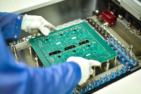
Stack-up design and lamination control are the foundation of qualified 12-layer tablet HDI boards. Most tablet motherboards adopt symmetric stack-up structure to avoid uneven internal stress. We strictly control layer alignment tolerance within ±0.03mm throughout production. Symmetric lamination is carried out at a constant temperature of 170–178°C and vacuum pressure of 2.0–2.5MPa. The whole cooling process is slowed to 3°C per minute, keeping final board warpage below 0.07%. This standard is far stricter than regular consumer PCBs, perfectly fitting the ultra-thin assembly requirements of tablet devices.
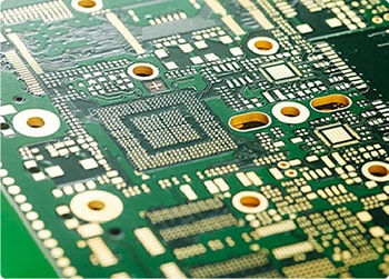
Microvia processing is the core difficulty in 12-layer HDI PCB manufacturing for tablet motherboards. A large number of fine-pitch BGAs and IC chips are densely arranged on tablet mainboards, requiring ultra-fine interlayer conduction. We use UV laser drilling to form microvias with a minimum diameter of 0.08mm. All vias undergo plasma desmear and full copper plating treatment, controlling the via defect rate below 2%. We also maintain the microvia aspect ratio within 0.8:1, effectively preventing via cracking and open circuit issues after long-term tablet operation and frequent screen switching.
Impedance stability and signal integrity are key to ensuring smooth tablet system operation. Tablet HDI boards carry high-speed DDR and display signal lines, which are very sensitive to transmission loss. We lock impedance tolerance at ±5% for all high-speed signal traces. During stack-up and routing optimization, we reasonably adjust dielectric thickness and copper foil thickness. This greatly reduces high-frequency signal crosstalk and attenuation, ensuring no screen flickering, touch delay or system stuttering caused by poor PCB signal transmission.
Thin-board process control is unique for tablet motherboard production. Most tablet 12-layer HDI PCBs require a finished board thickness of only 0.8mm to 1.0mm. We adopt low-profile 1067 and 1080 prepreg materials for lamination, ensuring uniform resin filling without layer voids or resin overflow. Strict surface treatment is implemented for ultra-thin boards to avoid board bending, copper exposure and thin-layer delamination, common defects in low-end thin HDI PCB production.
Reliability testing follows strict consumer electronics standards for all custom 12-layer HDI PCB for tablet motherboards. Every finished board undergoes 100% AOI optical inspection and full electrical conduction testing. We also perform batch sampling thermal cycling tests ranging from -30°C to 110°C, simulating daily portable usage scenarios. This eliminates hidden troubles such as unstable contact and intermittent circuit failure caused by temperature changes.