










Ball Grid Array (BGA) packaging is widely used in high-speed, high-density electronic designs. From communication equipment to automotive and computing applications, BGA enables large pin counts within a compact footprint. However, BGA is also one of the most demanding packages in PCBA manufacturing.
This article explains why BGA packaging is challenging, how it impacts PCB assembly, and what best practices are required to achieve reliable results.
What Is BGA Packaging?
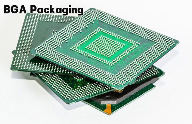
BGA components use an array of solder balls located underneath the package instead of traditional leads. During reflow soldering, these balls melt and form solder joints directly with PCB pads.
Compared to leaded packages, BGA offers:
Higher I/O density
Shorter electrical paths
Better signal integrity for high-speed designs
Key Manufacturing Challenges of BGA Assembly
1. Invisible Solder Joints
All BGA solder joints are hidden under the component after assembly. This means:
Visual inspection is impossible
Defects such as voids, bridges, or open joints cannot be detected by AOI alone
X-ray inspection is mandatory for reliable BGA assembly.
2. PCB Design Dependency
BGA performance is closely tied to PCB design quality:
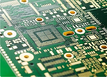
HDI structures (microvias, blind/buried vias) are often required
Pad design (NSMD vs SMD) affects solder joint reliability
Via-in-pad designs require proper filling and planarization
Poor PCB design can significantly reduce BGA yield, even with perfect assembly processes.
3. Reflow Profile Sensitivity
BGA solder balls are highly sensitive to:
Temperature ramp rate
Peak temperature
Time above liquidus
Uneven heating may result in head-in-pillow defects or incomplete solder wetting.
Best Practices for Reliable BGA PCBA
Perform DFM review before prototyping
Use X-ray inspection for all BGA assemblies
Control moisture sensitivity levels (MSL)
Validate reflow profiles during trial builds
Apply first article inspection (FAI) for new designs
Typical Applications of BGA Packaging
Networking and communication systems
Automotive electronics (ADAS, control units)
AI, computing, and embedded processing modules
BGA packaging is not just a component choice—it is a system-level manufacturing decision that requires experienced PCBA capabilities.