通用選擇器
僅限完全匹配
在標題中搜尋
在內容中搜尋
文章類型選擇器
  • 主頁
  • 品質
  • 博客
  • 聯絡 ANPSE

What is a HDI PCB?

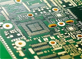
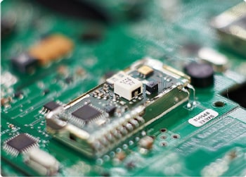
HDI PCB represents High Density Interconnect Printed Circuit Board. It is an advanced technology in multilayer circuit boards and are among the fastest-growing solutions in the industry. These boards sit on a high-density substrate with routing and pad connections compared to standard PCBs.

Designed for compact and high-performance applications, HDI PCBs feature significantly higher wiring density than conventional boards. They are typically based on a laminated structure with double-sided or multilayer cores, making them lighter, thinner, shorter, and smaller.

HDI technology enables greater miniaturization of electronic products while delivering enhanced performance and efficiency, meeting the demands of modern, high-tech designs.

Features of PCBAMake HDI PCB
If you are developing complex electronic products, you need durable, reliable, and high-performance HDI PCBs. With PCBAMake’s advanced HDI manufacturing capabilities, we deliver customized solutions tailored to your specific needs.
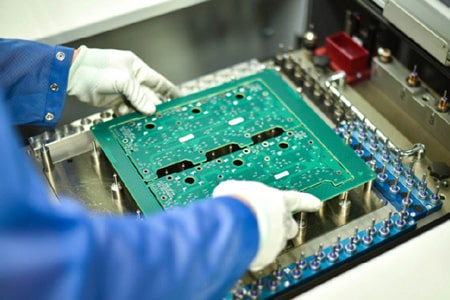
Since 1996, PCBAMake has been committed to supporting innovation and meeting the challenges of increasingly sophisticated technologies. One of our core values is uncompromising quality in every circuit board we produce. To ensure this, we apply rigorous quality control measures at every stage of the manufacturing process, including:
請聯絡我們以取得報價

  • Blind and/or buried vias
  • Min. Line Width/Space: 0.05/0.05mm
  • Via-in-pad
  • Through vias from surface to surface
  • 20 μm circuit geometries
  • 30 μm dielectric layers
  • 50 μm laser vias
  • 125 μm bump pitch processing
  • Surface Finish: ENIG/OSP/HASL/Au Plating (soft/hard)/ Immersion Ag/ Immersion Tin/ Bright Tin Plating/Ag Plating/Carbon Ink
PCBAMake HDI PCB
We're capable of manufacturing HDI PCB up to 40 layers in various structures, check the following table for our available HDI PCB structures:
HDI Structures Type of Microvias Mass Production Small /Middle Batch 原型 Layers Availible
1+N+1 Blind vias 是的 是的 是的 4 layers+
2+N+2 Blind/Buried staggered vias 是的 是的 是的 4 layers+
2+N+2 Blind/Buried stacked vias 是的 是的 是的 6 layers+
3+N+3 Blind/Buried staggered vias / 是的 是的 8 layers+
3+N+3 Blind/Buried Stacked Vias / / 是的 8 layers+
HDI PCB Capability
ITEM 能力
Layers 1-28
Thicker Copper 1-6OZ
Products Type HF(High-Frequency)&(Radio Frequency) board, Impedance controlled board , HDI board ,BGA& Fine Pitch board
阻焊層 Nanya&Taiyo ;LPI & Matt Red, green, yellow,white, blue,black.
Base material FR4(Shengyi China、ITEQ, KB A+,HZ), HI-TG, FR06, Rogers,Taconic、Argon、Nalco、Isola and so on
Finished Surface Conventional HASL,Lead-free HASL,Falsh Gold, ENIG (Immersion Gold)OSP(Entek), Immersion Tin,ImmersionSilver,Hard Gold
Selective Surface Treatment ENIG(immersion Gold)+OSP, ENIG(immersion Gold)+Gold Finger,Flash Gold +Gold Finger, immersion Silver+ Gold Finger, Immersion Tin+Gold Finger
Technical Specification Minimum line width/gap:3.5/4mil(laser drill)
Minimum hole size:0.15mm(mechanical drill)/4mil(laser drill)
Minimum Annular Ring: 4mil
Max Copper thickness: 6OZ
Max Production size:900×1200mm
Board Thickness:D/S: 0.2-7.0mm, Multilayers:0.40-7.0mm,
Min Solder Mask Bridge:0.08mm
Aspect ratio: 15:1
Plugging Visa capability: 0.2-0.8mm
寬容 Plated holes Tolerance:0.08mm(min±0.05)
Non-plated hole tolerance:0.05min(min+0/-0.05mm or +0.05/-0mm)
Outline Tolerance:0.15min(min±0.10mm)
Functional test :
Insulating resistance : 50 ohms (mormality)
Peel off strength: 1.4N/mm
Thermal Stress test :2650c,20 seconds
Solder mask hardness:6H
E-Test voltage :500V+15/-0V 30S
Warp and Twist: 0.7% (semiconductor test board≤0.3% )

HDI PCB Application

Consumer Electronics
醫療設備
醫療設備
Automotive Applications

Why Choose PCBAMake For Your HDI PCB?

Over 20 years of PCB experience
PCBAMake has been delivering high-density interconnect printed circuit boards for more than 20 years, and we believe no order is too small, and no tolerance is too tight. Pair that with competitive pricing, quick quotes and response times, domestic and offshore manufacturing and an unprecedented level of flexibility, and you have a winning combination for all your HDI PCB needs.
Benefits
Shorter PCB manufacturing time-to-market and enhanced machine performance for Flip Chip, BGA, MCM, SIP technologies.
Advanced technology
Ultra thin cores, fine line geometries and alternative via methods for improved thermal transfer for thermal PCBs. In compliance with 20um circuit geometries, 30um dielectric layers, 50um laser vias and 125um bump pitch processing.
Short delivery time
Allows reducing the lead times by combining the manufacturing capabilities with a profound understanding of high speed digital and high frequency RF package requirements.
Better design
Increases the area for PCB designer to place electronical components and also enhances faster signal transmission and reduced signal loss. Our high HDI PCB boards have the technology-driving capabilities to bring applications in a large number of industries including but not limited to semiconductor test equipment, military weapons, medical, and aerospace.
常見問題
Q
貴公司從事 PCB 與 PCBA 製造已有多久了?
A
PCBAMake 從事印刷電路板製造已超過 26 年。我們於 1996 年興建組裝廠並開始從事組裝業務。.
Q
如何快速取得 PCB 或 PCB 組裝的報價?
A
請將您的檔案及需求寄至 Orders@pcbamake.com. 待我們完成評估後,將立即回傳報價單。.
Q
貴公司是否提供 SMT 原型電路板的代工服務?
A
是的,我們具備完善的設備,能夠滿足您任何類型的客製化 SMT 試作板需求。最低訂購量為 10 片。.
Q
針對我的 PCBA 訂單,您需要哪些檔案和文件?
A
為確保組裝作業的準確性與效率,我們需要 Gerber 檔案、Excel 格式的物料清單 (BOM)、質心資料,以及(如有)組裝說明書。.

我能為您做些什麼呢?

電子郵件
信箱:666666@qq.com
電子郵件
電話:666666@qq.com
微信
WhatsApp 二維碼
WhatsApp
WhatsApp 二維碼
(0/8)