

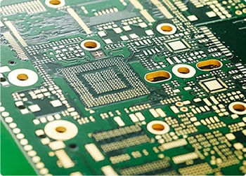
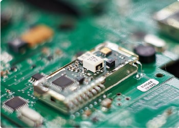
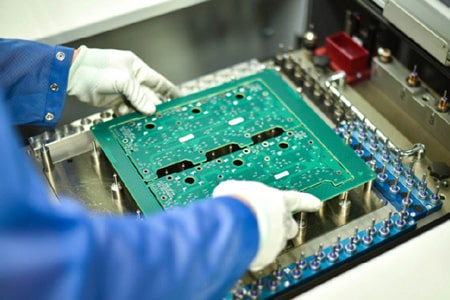
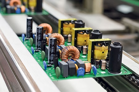










Any engineer designing HDI, high-speed, or automotive PCBs will run into the same via-in-pad question. When your layout requires vias sitting directly under component pads, leaving holes open is never a practical solution. To fix pad flatness issues and boost long-term board reliability, PCB fabricators mainly use two proven methods: Electroplated Blind Via Fill and resin plugging. These two processes often get mixed up, even by experienced designers. Picking the wrong one can hurt signal integrity, restrict current handling, or simply waste budget on unnecessary premium processes. While both techniques seal microvias and support standard via-in-pad layouts, their material properties, electrical behavior, manufacturing requirements and best-use cases are vastly different. Getting this selection right makes a huge difference in final PCB performance and production yield.
Electroplated Blind Via Fill is an advanced electroplating process exclusive to high-end HDI PCB builds. Instead of covering vias with ink or filling them with insulating material, manufacturers fully pack the entire via cavity with pure electrolytic copper. The plated copper matches the base board’s copper characteristics perfectly. After precision plating and mechanical planarization, the finished vias are completely flat, solid, and fully conductive from top to bottom.
正是这种实心铜结构,使得该工艺独具特色。过孔内部没有空隙,因此垂直信号和电流流动不会遇到任何阻抗不连续现象。对于高速数字线路和微波电路而言,这意味着更低的插入损耗、更稳定的阻抗控制以及更优异的信号完整性。 此外,铜填充过孔还具备卓越的载流能力,这对需要稳定供电的高功率密度HDI设计至关重要。.
树脂封孔的工作原理则截然不同。它使用非导电环氧树脂填充空的过孔。该工艺并非用于建立电气连接,其主要作用是绝缘、密封孔洞以及提高表面平整度以利于组装。 树脂固化后,会将过孔紧密封堵,阻止焊料通过孔洞渗入,并防止在SMT回流焊接过程中出现焊球缺陷。它能形成均匀的焊盘表面,非常适合标准BGA和细间距元器件。.
需要注意的是,树脂填充的过孔无法导电。 环氧树脂层将过孔的顶部和底部铜层完全隔离,切断了任何垂直的导电路径。由于这一限制,树脂填充技术绝不会用于有源信号过孔或电源过孔。它仅适用于密封虚拟过孔以及仅需平整度和绝缘保护的非功能性焊盘内过孔位置。.
Manufacturing difficulty and cost are also key decision factors. Electroplated Blind Via Fill requires multi-step precision electroplating, strict current tuning, and post-plating planarization. It needs tight process control to maintain good yield, which inevitably raises production costs. Only experienced high-end PCB manufacturers can deliver stable, consistent copper filling quality for mass production.
如果您的主要目标是过孔绝缘、提高SMT装配良率以及以经济高效的方式实现焊盘平整度,请选择树脂填充工艺。该工艺在消费类电子产品、基于标准BGA的PCB以及具有常规可靠性要求的中密度电路中均能可靠地发挥作用。.