

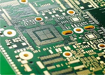
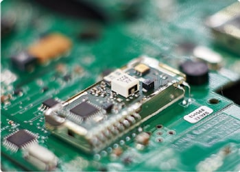
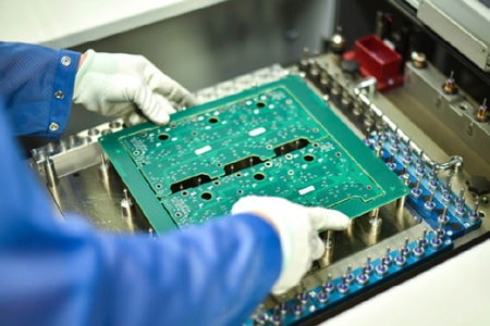
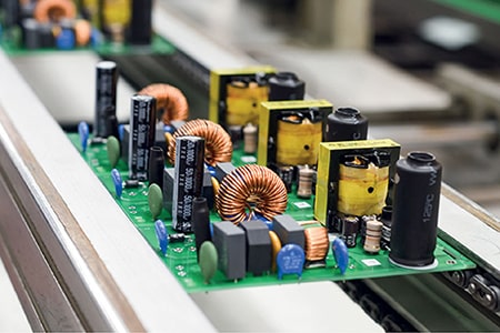










A high aspect ratio IC test board is a specialized precision PCB built for semiconductor chip testing and performance verification. Unlike standard circuit boards, custom IC test boards require ultra-precise fabrication, especially in complex hole processing. It serves as a critical connection carrier between IC chips and ATE testing equipment, delivering stable and accurate test data for semiconductor research and mass production.
High aspect ratio drill hole processing is one of the biggest technical challenges for premium IC test boards. Most high-precision chip test scenarios require tiny drill holes with ultra-high depth-to-diameter ratios. Conventional PCB drilling processes easily cause broken drills, rough hole walls and inconsistent hole conductivity. Professional high aspect ratio IC test boards adopt refined drilling and desmear processes. This ensures smooth inner hole walls, complete copper plating and stable hole impedance, which avoids test signal deviation caused by defective hole structures.
Precise signal stability is another key feature of industrial IC test boards. These test PCBs apply strict impedance control and independent channel isolation design. The structure effectively suppresses high-frequency signal crosstalk and transmission loss. Most boards use thick immersion gold surface finishing. It provides ultra-smooth probe contact surfaces, resists oxidation, and guarantees repeated and stable probing for long-term batch IC testing.
Strong structural reliability adapts to continuous industrial test scenarios. Custom IC test boards with high aspect ratio holes adopt high-rigidity substrates and optimized multi-layer stacking structure. The design prevents board deformation and layer delamination under frequent probe pressure and repeated plugging. Optimized via layout and high-precision hole metallization greatly reduces testing failure rates, extending board service life and lowering overall semiconductor testing costs.
High-precision IC test boards with high aspect ratio drilling are widely used in the semiconductor industry. They support functional testing, parametric testing and burn-in reliability testing for high-pin-count and high-speed IC chips. They are commonly applied in automotive-grade IC verification, communication chip testing, consumer semiconductor inspection and new chip R&D debugging. With strict hole processing standards and stable electrical performance, these professional test boards have become essential accessories for high-precision semiconductor test systems.