

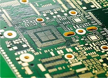
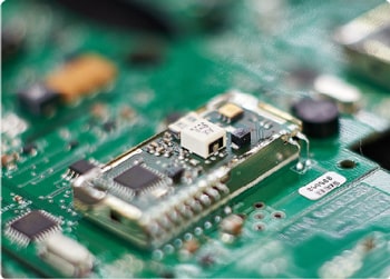










IoT module PCB acts as the core circuit carrier for miniature wireless communication and sensing devices in Internet of Things systems. Most compact wireless IoT modules adopt PCB castellated half-hole technology for surface mounting and board-to-board direct soldering, a design rarely seen on ordinary commercial PCBs. This unique edge half-hole structure eliminates the need for external connectors. It streamlines SMT assembly processes, greatly reduces the overall module footprint, and delivers better structural stability for low-power wireless IoT terminals that require compact size and high integration.
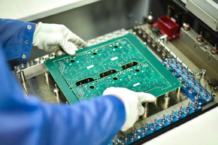
Based on actual PCB manufacturing practices, the production ofhalf-hole PCB for IoT modules follows a reversed and precise process flow, completely different from standard drilled hole fabrication. The whole procedure starts with standard through-hole drilling on raw PCB panels. Full electroless copper and electroplating processing is then performed to form complete conductive copper barrels inside each hole. After solder mask printing and ENIG surface finishing are fully completed, professional CNC routing equipment cuts precisely through the center of every plated hole. This step splits intact through holes into uniform semi-circular metalized edges, forming functional castellated half-holes for IoT module soldering and assembly.
Though castellated half-holes look structurally simple on drawings, they bring multiple technical challenges that directly impact mass production yield for high-precision IoT PCBs. Precision CNC routing control stands as the biggest difficulty. Even tiny positioning deviations during cutting can scratch internal hole copper layers, resulting in burrs, copper peeling and broken conductive paths. Uneven electroplating thickness is another common issue. It often causes partial copper loss after milling, which weakens solderability and leads to unstable electrical contact after module mounting. Furthermore, modern ultra-small IoT modules feature dense half-hole layouts with ultra-fine pitch spacing. This tight layout raises short-circuit risks and demands far stricter dimensional tolerance control throughout the entire PCB production process.
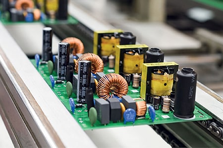
Benefiting from its miniaturized design and reliable soldering performance,castellated half-hole IoT PCB has become a mainstream solution for mass-produced wireless IoT hardware. It is widely applied in WiFi, Bluetooth, LoRa, and NB-IoT wireless communication modules used for consumer and industrial sensing. In smart home scenarios, these customized PCBs support miniaturized sensing terminals, human induction modules and intelligent control switch boards. For industrial IoT applications, they work steadily in low-power environmental monitoring equipment and remote data acquisition terminals, adapting perfectly to long-term, high-density and low-energy IoT deployment environments.